(Hong Kong)


Product Summary
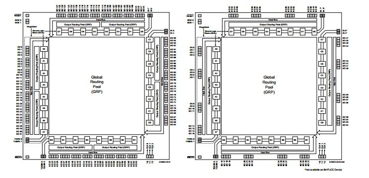
The ltn116at02-d01 is a High Density Programmable Logic Device available in 128 and 64 I/O-pin versions. The device contains 128 Registers, eight Dedicated Input pins, three Dedicated Clock Input pins, two dedicated Global OE input pins and a Global Routing Pool (GRP). The GRP provides complete interconnectivity between all of these elements. The ltn116at02-d01 features in-system programmability through the Boundary Scan Test Access Port (TAP) and is 100% IEEE 1149.1 Boundary Scan Testable. The ltn116at02-d01 offers non-volatile reprogrammability of the logic, as well as the interconnect to provide truly reconfigurable systems.
Parametrics
ltn116at02-d01 absolute maximum ratings: (1)Supply Voltage Vcc: -0.5 to +5.4V; (2)Input Voltage Applied: -0.5 to +5.6V; (3)Off-State Output Voltage Applied: -0.5 to +5.6V; (4)Storage Temperature: -65 to 150°C; (5)Case Temp. with Power Applied: -55 to 125°C; (6)Max. Junction Temp. (TJ )with Power Applied: 150°C.
Features
ltn116at02-d01 features: (1)SuperFAST HIGH DENSITY IN-SYSTEM PROGRAMMABLE LOGIC; (2)6000 PLD Gates; (3)128 and 64 I/O Pin Versions, Eight Dedicated Inputs; (4)128 Registers; (5)High Speed Global Interconnect; (6)Wide Input Gating for Fast Counters, State Machines, Address Decoders, etc.; (7)Small Logic Block Size for Random Logic; (8)100% Functional, JEDEC and Pinout Compatible with ispLSI 2128V Devices; (9)3.3V LOW VOLTAGE 2128 ARCHITECTURE; (10)Interfaces with Standard 5V TTL Devices; (11)HIGH PERFORMANCE E2 CMOS TECHNOLOGY; (12)fmax = 250MHz Maximum Operating Frequency; (13)tpd = 4.0ns Propagation Delay; (14)Electrically Erasable and Reprogrammable; (15)Non-Volatile; (16)100% Tested at Time of Manufacture; (17)Unused Product Term Shutdown Saves Power.
Diagrams