(Hong Kong)

Product Summary
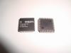
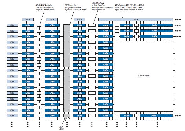
The EP2C35F672I8 is an FPGA. The device contains a two-dimensional row- and column-based architecture to implement custom logic. Column and row interconnects of varying speeds provide signal interconnects between logic array blocks (LABs). The EP2C35F672I8 is embedded memory blocks, and embedded multipliers. The low cost and optimized feature set of the EP2C35F672I8 make them ideal solutions for a wide array of automotive, consumer, communications, video processing, test and measurement, and other end-market solutions.
Parametrics
EP2C35F672I8 absolute maximum ratings: (1)Supply voltage: -0.5 to 1.8V; (2)Output supply voltage: -0.5 to 4.6V; (3)PLL supply voltage: -0.5 to 1.8V; (4)DC input voltage: -0.5 to 4.6V; (5)DC output current, per pin: -25 to 40 mA; (6)Storage temperature: -65 to +150℃; (7)Junction temperature: 125℃.
Features
EP2C35F672I8 features: (1)High-density architecture with 4,608 to 68,416 LEs; (2)Embedded multipliers; (3)Advanced I/O support; (4)Flexible clock management circuitry; (5)Device configuration; (6)Intellectual property.
Diagrams
| Image | Part No | Mfg | Description |  |
Pricing (USD) |
Quantity | ||||||
|---|---|---|---|---|---|---|---|---|---|---|---|---|
 |
 EP2C35F672I8 |
|
IC CYCLONE II FPGA 33K 672-FBGA |
Data Sheet |
|
|
||||||
 |
EP2C35F672I8N |
|
IC CYCLONE II FPGA 33K 672-FBGA |
Data Sheet |
|
|
||||||