(Hong Kong)

Product Summary
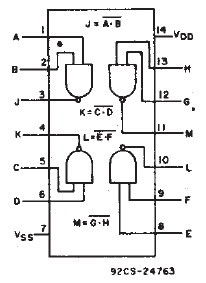
The CD4023BF is a CMOS NAND gate. It provides the system designer with direct implementation of the NAND function and supplement the existing family of CMOS gates. All inputs and outputs are buffered. The CD4023BF is supplied in 14-lead hermetic dual-in-line ceramic packages, and 14-lead thin shrink small-outline packages. It also is supplied in 14-lead thin shrink small-outline packages.
Parametrics
CD4023BF absolute maximum ratings: (1)DC supply-voltage range(VDD)voltage referenced to VSS terminal: -0.5V to +20V; (2)Input voltage range all inputs: -0.5V to VDD+0.5V; (3)DC input current, any one input: ±10mA; (4)Power dissipation per package(PD) for TA=-55℃ to 100℃: 500mW; for TA=+100℃ to +125℃: derate linearity at 12mW/℃ to 200mW; (5)Device dissipation per output transistor for TA=full package-temperature range(all package types): 100mW; (6)Operating temperature range(TA): -55℃ to +125℃; (7)Storage temperature range(Tstg): -65℃ to +150℃.
Features
CD4023BF features: (1)Propagation delay time=60ns(typ)at CL=50PF, VDD=10V; (2)Buffered inputs and outputs; (3)Standardized symmetrical output characteristics; (4)Maximum input current of 1μA at 18V over full package temperature range: 100nA at 18V and 25℃; (5)100% tested for quiescent current at 20V; (6)5V, 10V and 15V parametric ratings; (7)Meets all requirements of JEDEC tentative standard NO.13B, standard specifications for description of B series CMOS devices.
Diagrams
 |
 CD4000B |
Other |
|
Data Sheet |
Negotiable |
|
||||
|
CD4000BMS |
Other |
|
Data Sheet |
Negotiable |
|
||||
|
CD4001BC |
Other |
|
Data Sheet |
Negotiable |
|
||||
 |
CD4001BCM |
|
IC GATE NOR BUFF QUAD 2IN 14SOIC |
Data Sheet |
Negotiable |
|
||||
|
CD4001BCMX |
|
IC GATE NOR QUAD 2INPUT 14-SOIC |
Data Sheet |
Negotiable |
|
||||
 |
CD4001BCN |
|
IC GATE NOR BUFF QUAD 2IN 14-DIP |
Data Sheet |
Negotiable |
|
||||