Product Summary
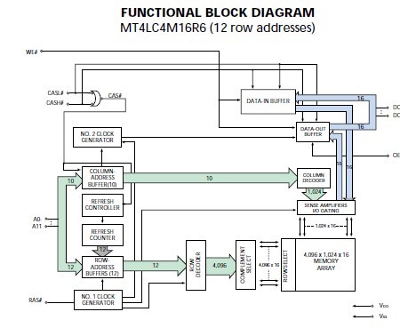
The 4 Meg x 16 DRAM MT4LC4M16R6TG-5F is a high-speed CMOS, dynamic random-access memory device containing 67,108,864 bits and designed to operate from 3V to 3.6V. The MT4LC4M16R6TG-5F is functionally organized as 4,194,304 locations containing 16 bits each. The 4,194,304 memory locations are arranged in 4,096 rows by 1,024 columns on the MT4LC4M16R6TG-5F. During READ or WRITE cycles, each location is uniquely addressed via the address bits: 12 row-address bits (A0-A11) and 10 column-address bits (A0-A9) on the MT4LC4M16R6TG-5F. In addition, both byte and word accesses are supported via the two CAS# pins (CASL# and CASH#).
Parametrics
MT4LC4M16R6TG-5F absolute maximum ratings: (1)Voltage on VCC Relative to VSS: -1V to +4.6V; (2)Voltage on NC, Inputs or I/O Pins Relative to VSS: -1V to +4.6V; (3)Operating Temperature, TA (ambient) Commercial: 0℃ to +70℃; (4)Extended (IT): -40℃ to +85℃; (5)Storage Temperature (plastic): -55℃ to +150℃; (6)Power Dissipation: 1W.
Features
MT4LC4M16R6TG-5F features: (1)Single +3.3V ±0.3V power supply; (2)Industry-standard x16 pinout, timing, functions, and package; (3)12 row, 10 column addresses (R6); (4)High-performance CMOS silicon-gate process; (5)All inputs, outputs and clocks are LVTTL-compatible; (6)Extended Data-Out (EDO) PAGE MODE access; (7)4,096-cycle CAS#-BEFORE-RAS# (CBR) REFRESH distributed across 64ms; (8)Optional self refresh (S) for low-power data retention.
Diagrams

 |
 MT4LC16M4A7 |
 Other |
 |
 Data Sheet |
 Negotiable |
|
||||
 |
 MT4LC16M4G3 |
 Other |
 |
 Data Sheet |
 Negotiable |
|
||||
 |
 MT4LC16M4H9 |
 Other |
 |
 Data Sheet |
 Negotiable |
|
||||
 |
 MT4LC16M4T8 |
 Other |
 |
 Data Sheet |
 Negotiable |
|
||||
 |
 MT4LC1M16C3 |
 Other |
 |
 Data Sheet |
 Negotiable |
|
||||
 |
 MT4LC1M16E5 |
 Other |
 |
 Data Sheet |
 Negotiable |
|
||||
 (Hong Kong)


