(Hong Kong)

Product Summary
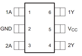
The SN74LVC2G34DBVR is a dual buffer gate. The SN74LVC2G34DBVR is designedfor 1.65-Vto 5.5-V VCC operation. The SN74LVC2G34 performs the Boolean function Y=Ain positive logic. The SN74LVC2G34DBVR is fully specified for partial-power-down applications using Ioff.
Parametrics
SN74LVC2G34DBVR absolute maximum ratings: (1) Supply voltage range Vcc: -0.5 to 6.5V; (2) Input voltage range VI: -0.5 to 6.5V; (3) Voltage range applied to any output in the high-impedance or power-off state Vo: -0.5 to 6.5V; (4) Voltage range appliedto any output in the high or low state Vo: -0.5 to Vcc +0.5V; (5) Input clamp current IIK: -50mA (VI<0) ; (6) Output clamp current: -50mA (Vo<0) ; (7) Continuous output current: ±50mA; (8) Continuous current through VCC or GND: ±100mA; (9) Storage temperature range Tstg: -65 to 150°C.
Features
SN74LVC2G34DBVR features: (1) Available in the Texas Instruments Nanofree Package; (2) Supports 5-V Vcc Operation; (3) Inputs Accept Voltages to 5.5V; (4) Max tpd of 4.1ns at 3.3V; (5) Low Power Consumption, 10-µA Max ICC; (6) ±24mA Output Drive at 3.3V; (7) typical VOLP (Output Ground Bounce) <0.8V at VCC=3.3V, TA=25°C; (8) Latch-Up Performance Exceeds 100mA Per JESD78, ClassII; (9) ESD Protection Exceeds JESD22: 2000-V Human-Body Model (A114-A) , 200-V Machine Model (A115-A) , 1000-V Charged-Device Model (C101) .
Diagrams
| Image | Part No | Mfg | Description |  |
Pricing (USD) |
Quantity | ||||||||||||
|---|---|---|---|---|---|---|---|---|---|---|---|---|---|---|---|---|---|---|
 |
 SN74LVC2G34DBVR |
Texas Instruments |
Buffers & Line Drivers Dual |
Data Sheet |
|
|
||||||||||||
|
SN74LVC2G34DBVRE4 |
Texas Instruments |
Buffers & Line Drivers 10-Bit FET Bus-Exchange Switch |
Data Sheet |
|
|
||||||||||||
|
SN74LVC2G34DBVRG4 |
Texas Instruments |
Buffers & Line Drivers Dual Buffer Gate |
Data Sheet |
|
|
||||||||||||