(Hong Kong)

Product Summary
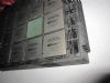
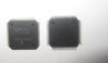
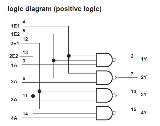
The SN75365N is a quadruple NAND interface circuit, which is designed to drive power MOSFETs from TTL inputs. It provides the high current and voltage necessary to drive large capacitive loads at high speeds. The outputs of SN75365N can be switched very close to the VCC2 supply rail when VCC3 is about 3 V higher than VCC2. VCC3 can also be tied directly to VCC2 when the source voltage requirements are lower. The SN75365N is characterized for operation from 0℃ to 70℃.
Parametrics
SN75365N absolute maximum ratings: (1)Supply voltage range of VCC1: –0.5 V to 7 V; (2)Supply voltage range of VCC2: –0.5 V to 25 V; (3)Supply voltage range of VCC3: –0.5 V to 30 V; (4)Input voltage, VI: 5.5 V; (5)Peak output current, II (tw < 10 ms, duty cycle < 50%): 500 mA; (6)Operating free-air temperature range, TA: 0℃ to 70℃; (7)Storage temperature range, Tstg: –65℃ to 150℃; (8)Lead temperature 1,6 mm (1/16 inch) from case for 10 seconds: 260℃.
Features
SN75365N features: (1)Quadruple Circuits Capable of Driving High-Capacitance Loads at High Speeds; (2)Output Supply Voltage Range From 5 V to 24 V; (3)Low Standby Power Dissipation; (4)VCC3 Supply Maximizes Output Source Voltage.
Diagrams
 |
 SN75061 |
Other |
|
Data Sheet |
Negotiable |
|
||||||||||||
|
SN75076B |
Other |
|
Data Sheet |
Negotiable |
|
||||||||||||
|
SN75107A |
Other |
|
Data Sheet |
Negotiable |
|
||||||||||||
 |
SN75107AD |
Texas Instruments |
Bus Receivers Dual Line |
Data Sheet |
|
|
||||||||||||
|
SN75107ADE4 |
Texas Instruments |
Buffers & Line Drivers DUAL LINE RECEIVER |
Data Sheet |
|
|
||||||||||||
|
SN75107ADG4 |
Texas Instruments |
Buffers & Line Drivers Dual Line Receiver |
Data Sheet |
|
|
||||||||||||